




















Asahi Kasei develops photosensitive PI film for advanced semiconductor packaging

Panel-level packaging has gained momentum in the semiconductor industry as manufacturers pursue higher efficiency and improved yield that can support next-generation packaging processes.
In response to these market changes, Asahi Kasei has combined the features of its photosensitive polyimide (PSPI) and dry film photoresist (DFR) into a new photosensitive film.

Asahi Kasei’s newly developed PSPI film.
The PSPI film is currently under customer evaluation, with commercial availability expected in the near future.
Easier lamination process
The new PSPI film was developed by combining Asahi Kasei’s expertise in the manufacture of PIMEL liquid PSPI used for buffer coatings and passivation layers and SUNFORT dry film photoresist for temporary lithographic circuit patterning on substrates and wafers.
It will improve productivity in semiconductor packaging manufacturing by enabling easy, uniform application of a lamination process to large square panels. In addition, the film is designed to accommodate an increased number of insulating layers.
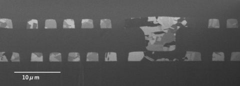
Cross-section of a redistribution layer formed with PSPI film and SUNFORT TA series.
The PSPI film is expected to be applied to redistribution layers for semiconductor packaging and insulating layers for package substrates.
More applications
By combining the new PSPI film with the SUNFORT TA series (capable of forming 1.0 μm-wide circuits), both fine circuit patterns and insulating resin layers can be formed by film lamination.
Asahi Kasei is also developing solutions that combine the PSPI film with the SUNFORT CX series, enabling the formation of high-aspect-ratio copper pillars required for three-dimensional semiconductor packaging.
Electronics as First Priority business in Asahi Kasei’s management plan
Electronics is positioned as a First Priority business in Asahi Kasei’s medium-term management plan Trailblaze Together. Electronic materials such as PIMEL PSPI and SUNFORT dry film photoresist are used in advanced semiconductor packaging applications.
| Semiconductor packaging process materials | Asahi Kasei products | |
| Liquid process (spin / slit coating) | Redistribution layer insulation | PIMEL photosensitive polyimide (PSPI) |
| Photoresist for wiring and copper pillars | - | |
| Film process (lamination) | Redistribution layer insulation | PSPI film (new) |
| Photoresist for wiring and copper pillars | SUNFORT dry film photoresist | |
Asahi Kasei’s products for semiconductor packaging.
Demand continues to rise as more chips are packaged at higher density and interposers become larger to meet the requirements of AI data centers. Wiring patterns are becoming finer and the number of layers is increasing as packaging transitions from wafer-level to panel-level, and becomes more 3-dimensional, further raising the performance requirements of packaging materials.