















Analysis: Japan’s chemical giants bet big on semiconductor and AI materials

Recently, a shift is observed in chemicalmaterial industry: the supply of high-end materials for semiconductor and AI is restructuring. When the majority is following updates from European and American companies, three chemical giants from Japan are undergoing a strategic planning from upstream to downstream.
The three Japanese companies – Mitsubishi Chemical, Sumitomo Chemical, and Asahi Kasei – have been reported with regular movement including concentrating R&D on new products, accelerating customer verification, and expanding productivity. They all focus on materials for high-end semiconductor, AI calculation, and data center.
In Asia, the race on developing materials for AI semiconductor has become a hard core competition among chemical companies.
Jumping out of the red ocean
The traditional chemical industry has already collapse into the deadlock of involution and limited profitability. Forward-thinking companies are planning on developing out of the red ocean.
Following the scaled implementation of AI server, continuous expansion of data center, and the rapid upgrading of advanced packaging technologies for semiconductor, high-end E&E materials have become a key in business transformation. The three Japanese chemical giants have invested in these business segments to respond to the hot trend of AI semiconductor.
Development focus of the Japanese chemical giants:
• Mitsubishi Chemical has made “empowering advanced data processing and communication” as the core development direction.
• Asahi Kasei has listed electronics business as the highest priority in its mid-term operation plan. This move signifies the company’s strategy in placing AI semiconductor materials in higher position that determines company’s future development.
Mitsubishi Chemical: Tackling the core challenge in high-end packaging
High-end, high-density chip packaging has faced two major challenges: thermal expansion and warpage, which are also bottlenecks for achieving higher yield rate of high-end chips.
Tackling these industry pain points, Mitsubishi Chemical has developed the negative thermal expansion filler “M-Filleris NTE”. The company also planned to sell pilot products by the end of FY2026, launch sales of mass produced products in the second half of FY2027, and offer masterbatches mixed with epoxy resin to significantly reduce development cost for downstream customers.
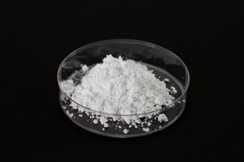
Negative thermal expansion filler. (Source: Mitsubishi Chemical)
Furthermore, in response to the stringent requirement of chemical mechanical polishing (CMP) for AI chips, Mitsubishi Chemical is building a new production facility for colloidal silica at its Kyushu Plant in Fukuoka, Japan. The facility is expected to start operation in October 2028.
Sumitomo Chemical: Restructuring manufacturing logic in semiconductor parts
The present development trend of semiconductor parts goes towards lightweight, precise, and structural complicated. Traditional injection molding technology can hardly fulfil these high-end manufacturing requirements.
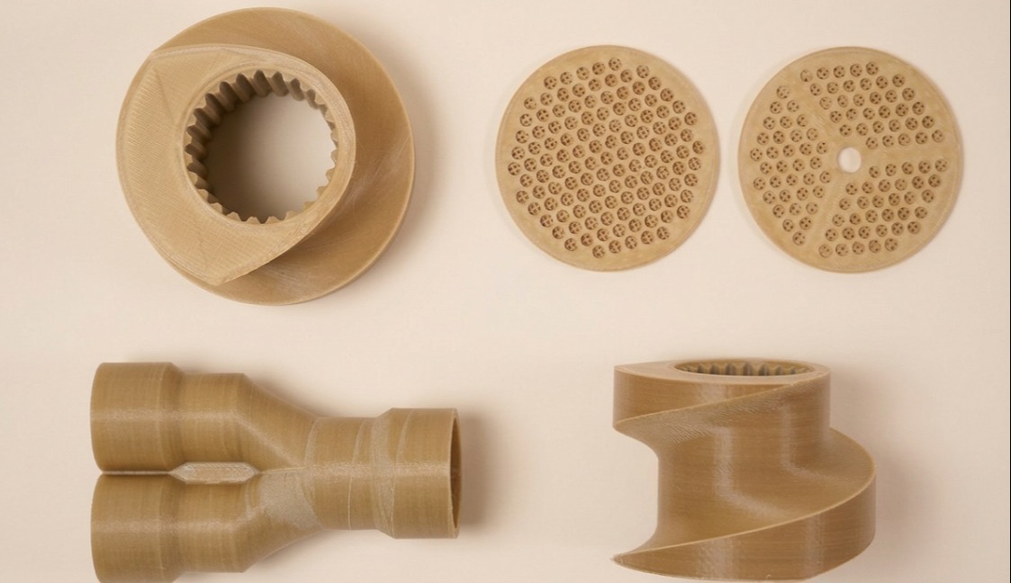
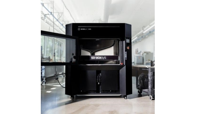
Aiming at this technology gap, Sumitomo Chemical collaborated with Gutenberg Co., Ltd. to develop a liquid crystal polymer (LCP) filament and molding technology for 3D printers that use the FFF method, and plan to begin providing samples of this filament in 2026.
This new material makes it possible to create complex shapes that are difficult to achieve with injection molding. Its application goes beyond semiconductor parts and can also covers high-end sectors including humanoid robot and aerospace.
Asahi Kasei: Deeply engaging in lithographic and insulating materials
Asahi Kasei is deeply engaged in the development of lithographic and insulating materials.
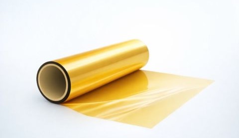
Combining the feature of photosensitive polyimide (PSPI) and dry film photoresist (DFR), Asahi Kasei has developed a new photosensitive film. It enables uniform application of a lamination process to large square panels and increased number of insulating layers. The PSPI film is currently under customer evaluation.
Meanwhile, Asahi Kasei invested US$12 million to build a new slitting facility for SUNFORT DFR at its manufacturing site in Taiwan, which will expand capacity by 40%. This further seizes the market share of high-end packaging lithographic materials and consolidates its own supply advantage.
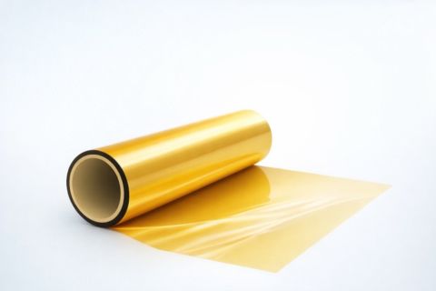
Asahi Kasei introduced new photosensitive film for semiconductor packaging. (Source: Asahi Kasei)
Upgrading layout logic
Some view Japanese companies as comparatively conservative. However, these three Japanese companies break the traditional lag mode of “R&D first, implementation later, and expansion at last”.
They all adopt the parallel move with upgrading technology and expanding capacity at the same time. With this mode, the companies can catch up with the peak time of rising in global AI semiconductor in 2026-2028.
Their layout logic is clear:
1. R&D: Develop for tackling pain points
R&D of all new products are based on the processing challenges in advanced packaging in real life. Every product tackles downstream manufacturing pain points.
2. Customer-end: Offering comprehensive solution
Apart from single material, the companies offer comprehensive solution combining core material and specialized equipment. This binds customers along the industry chain and increases customer stickiness.
3. Manufacturing-end: Plan for expanding capacity
Sample delivery, customer verification, and mass production are carried out accordingly. To have full control in supply chain, the companies also plan sufficiently ahead for capacity expansion.
Competition goes beyond technology
As the trend of AI semiconductor materials continues to rise, global chemical leaders expand their business layout in this sector, accelerating industry competition.
From the strategic layout of the three Japanese chemical leaders, we can see that industry competition is no longer limited in single technology or product – the competition focus is shifted to the integrated ability in core technology, integrated services, stability of production capacity, and forecasting ability in industry cycle.